
IBM's Chip Milestone Gets Expert Backing
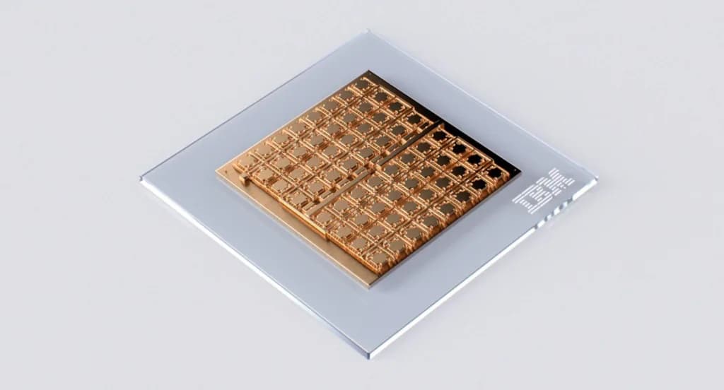
IBM has unveiled what it calls the world's first sub-1nm semiconductor chip, but the company's biggest achievement may not be the number attached to it. Instead, researchers are paying closer attention to how the chip is built. The prototype, known as the 0.7nm or 7 angstrom node, packs almost 100 billion transistors onto a chip
IBM's Chip Milestone Gets Expert Backing
IBM has unveiled what it calls the world’s first sub-1nm semiconductor chip, but the company’s biggest achievement may not be the number attached to it. Instead, researchers are paying closer attention to how the chip is built. The prototype, known as the 0.7nm or 7 angstrom node, packs almost 100 billion transistors onto a chip about the size of a fingernail. IBM says that’s roughly twice the transistor density of the 2nm chip it revealed in 2021. If it reaches production, the design could offer up to 50% more computing performance or reduce power consumption by as much as 70%. Prof Francesco Petruccione, director of the National Institute for Theoretical and Computational Sciences (NITheCS) and professor of quantum computing at Stellenbosch University, said the announcement shows there is still room to improve conventional chip technology.
“This is an important engineering milestone. It shows that chip manufacturers are still finding ways to make computer chips more powerful and more energy-efficient, despite many experts believing that traditional scaling was approaching its limits. “Chip manufacturers have spent decades shrinking transistors to squeeze more of them onto a piece of silicon. That approach is becoming harder with every new generation. IBM has chosen a different direction. Rather than depending only on smaller transistors, its new “nanostack” design places them on top of one another in multiple layers. The result is a denser chip without relying entirely on further miniaturisation. “The real innovation is not simply making transistors smaller, but redesigning how they are arranged in three dimensions,” Petruccione said. He also noted that process names such as 2nm and 0.7nm are no longer literal measurements of transistor size. Today they mainly distinguish one manufacturing generation from the next.
Where users could notice the difference
The benefits won’t arrive overnight. IBM’s design is still a research prototype, and commercial production is years away. If it reaches the market, consumers are likely to notice improvements in battery life, processing speed and the ability to run more AI features directly on their devices. “It could eventually translate into faster smartphones and laptops, longer battery life and more capable AI assistants running directly on devices,” Petruccione said. Businesses running large data centres stand to gain too. “The bigger impact is likely to be lower energy costs in data centres and the ability to process much larger AI workloads, making advanced AI applications more affordable and widely available.”
AI is pushing chipmakers in a new direction
The rapid growth of artificial intelligence has changed what chip designers need to prioritise. Training modern AI models demands huge amounts of computing power and electricity. That has made power efficiency almost as important as raw performance. “AI progress increasingly depends not only on better algorithms but also on better hardware,” Petruccione said. IBM also says it has increased the density of on-chip SRAM by about 40%. While less eye-catching than transistor counts, that improvement matters because AI systems constantly move data between processors and memory. Keeping more of that memory on the chip reduces delays and cuts energy use.
The brain comparison only goes so far
IBM’s 100 billion transistors inevitably invite comparisons with the roughly 86 billion neurons in the human brain. Petruccione says that comparison oversimplifies things. The brain’s real complexity lies in the estimated 100 trillion synapses linking those neurons together. Unlike transistors, those connections strengthen, weaken and reorganise continuously. Modern AI systems are measured differently again. Their scale is based on parameters rather than transistors, and the largest models already contain trillions of them. Chips like IBM’s won’t suddenly produce human-level intelligence. What they can do is lower the cost of running increasingly demanding AI systems.
South Africa’s role
Petruccione does not expect South Africa to become a manufacturer of cutting edge semiconductors. He argues the country’s strengths lie elsewhere. “We can build expertise in designing AI algorithms, developing software, quantum computing, quantum technologies and high-performance computing.” That, he says, is where investment should go if South Africa wants to remain competitive as computing continues to advance. He also urged caution over IBM’s timeline. The prototype is a research achievement, but moving from a laboratory demonstration to mass production remains one of the biggest hurdles in the semiconductor industry. IBM believes production could begin within five years. Petruccione said that timeframe is possible, although considerable engineering and commercial work still lies ahead.